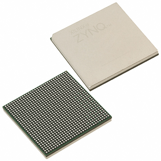
XC7K325T-2FFG900I,XILINX,High Performance Embedded Field Programmable Gate Arrays

The XC7K325T-2FFG900I from Xilinx represents a cutting-edge FPGA designed for high-performance applications. Its advanced architecture includes 325,000 logic cells, 840 DSP slices, and 2,700 Kb of block RAM, making it a powerful choice for demanding tasks.
Feature | Specification |
|---|---|
Logic Cells | 325,000 |
DSP Slices | 840 |
Block RAM | 2,700 Kb |
I/O Pins | 900 |
Operating Frequency | Up to 550 MHz |
Operating Temperature | -40°C to +100°C |
This FPGA leverages 28nm process technology to deliver higher logic density and faster processing speeds. You can use it for applications like digital signal processing, embedded systems, and AI acceleration. Its dedicated DSP slices enhance performance in filtering, modulation, and other signal analysis tasks, ensuring efficient and reliable designs.
Key Takeaways
The XC7K325T-2FFG900I FPGA has 325,000 logic cells and 840 DSP slices. It works well for tasks like AI and signal processing.
Use the Xilinx Vivado Design Suite to make FPGA development easier. It includes tools for checking timing, saving power, and fixing problems quickly.
Try power-saving methods like clock gating to use less energy. This helps the FPGA work better and more efficiently.
Follow modular design steps to make your FPGA projects simpler. This makes it easier to change or grow as needed.
Use the FPGA's many input/output options and PCIe support. These features help connect to other devices and move data quickly.
Overview of XC7K325T-2FFG900I
Key Specifications
Logic cells, DSP slices, and block RAM
The XC7K325T-2FFG900I offers a robust architecture tailored for high-performance applications. With 325,000 logic cells, 840 advanced DSP slices, and 2,700 Kb of block RAM, this field-programmable gate array provides the resources you need for complex designs. These specifications make it ideal for tasks like digital signal processing and AI acceleration.
Specification | Value |
|---|---|
Logic Cells | 325,000 |
DSP Slices | 840 |
Block RAM | 2,700 Kb |
Operating Frequency | Up to 550 MHz |
I/O Pins | 900 |
Operating Temperature Range | -40°C to +100°C |
I/O capabilities and PCIe support
This FPGA supports 900 I/O pins, enabling seamless interfacing with external devices. Its PCIe support ensures high-speed data transfer, making it suitable for applications requiring rapid communication and data routing. These features enhance its flexibility for use in telecommunications and embedded systems.
Feature | Description |
|---|---|
I/O Pins | Supports 900 I/O pins for interfacing with external devices. |
Power efficiency and thermal management
The XC7K325T-2FFG900I incorporates dynamic power management features to optimize energy usage. Techniques like clock gating and low-power modes reduce power consumption when certain sections are idle. You can also use tools like the Vivado Power Analyzer to identify and address power-hungry areas. These capabilities ensure efficient operation and effective thermal management, even in demanding environments.
Dynamic power management reduces energy usage during idle states.
Clock gating minimizes power consumption in unused sections.
Low-power modes allow unused logic blocks to power down.
Resource optimization lowers overall power consumption.
Features for High-Performance FPGA Design
Scalability and flexibility for complex designs
This FPGA provides a flexible configuration that adapts to your design needs. Its extensive logic resources and abundant I/O options allow you to scale your projects efficiently. Whether you're working on industrial automation or high-speed communication systems, the XC7K325T-2FFG900I ensures seamless scalability.
High-speed data processing and low latency
The XC7K325T-2FFG900I excels in high-speed processing, thanks to its advanced DSP capabilities and multiple high-speed transceivers. These features enable low-latency performance, making it perfect for applications like digital signal processing and real-time computing. Its 28nm process technology further enhances processing speed and efficiency.
Cost-effectiveness compared to ASICs
This FPGA offers significant cost advantages over ASICs. Its lower initial costs and flexibility in design changes reduce your time-to-market. Additionally, its energy-efficient design contributes to lower operating expenses. With the best price/performance/watt at 28nm, the XC7K325T-2FFG900I delivers exceptional value for high-performance capabilities.
Lower initial costs and faster time-to-market.
Energy-efficient design reduces operating expenses.
Cost-effective packaging and high DSP ratios.
Preparing for Design with XC7K325T-2FFG900I
Tools and Software
Overview of Xilinx Vivado Design Suite
The Xilinx Vivado Design Suite is your go-to tool for developing with the XC7K325T-2FFG900I. It provides a comprehensive environment for FPGA development, offering features that simplify the design process. You can use its Integrated Logic Analyzer (ILA) to debug internal FPGA signals in real time. Timing analysis tools help ensure your design meets performance requirements, while power analysis tools allow you to estimate and optimize power consumption.
To get started, follow these steps:
Use an XDC file to define timing constraints for your design.
Analyze timing reports to identify critical paths and resolve timing violations.
Run power analysis to optimize your design's energy efficiency.
Vivado also includes simulation, programming, and debugging capabilities, ensuring your FPGA design is both functional and reliable.
Additional tools for simulation and debugging
Beyond Vivado, other tools enhance your development workflow. Timing Analyzer identifies timing violations and suggests fixes, while the Power Analyzer estimates power consumption. The CDC Checker ensures proper functionality by analyzing clock domain crossings. These tools work together to improve the efficiency and reliability of your FPGA designs.
Tool | Purpose |
|---|---|
Xilinx Vivado Design Suite | Comprehensive design environment for FPGA development. |
Timing Analyzer | Identifies timing violations and suggests fixes. |
Power Analyzer | Estimates and optimizes power consumption. |
CDC Checker | Analyzes clock domain crossings to ensure proper functionality. |
Development Environment Setup
Hardware requirements and board setup
To begin, ensure you have the necessary hardware. A development board compatible with the XC7K325T-2FFG900I is essential. Connect the board to your computer using a USB or JTAG cable. Verify that your power supply meets the board's requirements to avoid instability during operation.
Configuring Vivado for XC7K325T-2FFG900I
Once your hardware is ready, configure Vivado for the XC7K325T-2FFG900I. Start by creating a new project and selecting the correct FPGA part number. Import your design files and define constraints using an XDC file. Use Vivado's timing and power analysis tools to refine your design for optimal performance.
Initializing and testing the FPGA
Testing ensures your FPGA operates as intended. Use diagnostic tools like ChipScope and Vivado to monitor the FPGA's behavior. Minimize logic usage by employing efficient coding practices and optimizing timing to meet critical path requirements. Partition your design into smaller sections for better management. Conduct thorough simulations before deploying your design to the hardware.
Tip: Implement power management techniques like clock gating to enhance energy efficiency during testing and operation.
Best Practices for Efficient FPGA Design
Resource Optimization
Efficient use of logic, memory, and routing
Optimizing resources in FPGA designs ensures better performance and reliability. You can achieve this by employing strategies like logic partitioning and clustering. Identify natural hierarchies in your design and group related functions together. Timing-driven placement also plays a crucial role. Incorporate timing information into the placement process to minimize delays and improve efficiency. Additionally, utilize FPGA-specific resources such as block RAM and DSP slices to maximize the potential of the XC7K325T-2FFG900I.
Other techniques include:
Using functional clustering algorithms based on connectivity.
Refining placement iteratively based on timing analysis.
Leveraging routing and placement strategies to reduce congestion.
Power optimization techniques
Efficient power management is critical for FPGA designs. The XC7K325T-2FFG900I offers features like clock gating to reduce power consumption. Lowering the clock frequency can also help when high speed is unnecessary. Transition unused logic blocks to low-power modes or idle states to conserve energy. Tools like the Vivado Power Analyzer allow you to identify power-hungry areas and optimize them effectively.
Additional tips include:
Choosing lower-voltage I/O standards.
Minimizing the number of active logic elements.
Optimizing routing to reduce unnecessary power usage.
High-Performance Architectures
Pipelining and parallelism for speed
Pipelining enhances the performance of FPGA designs by enabling concurrent processing of multiple data items. This technique ensures that new inputs are processed every cycle, maximizing hardware utilization. By breaking down processes into smaller segments, pipelining reduces the critical path length, leading to faster execution times. Parallelism further boosts performance by allowing multiple operations to run simultaneously. These methods leverage the advanced DSP capabilities of the XC7K325T-2FFG900I for high-speed data processing.
Modular design for scalability
Modular design simplifies scalability in FPGA projects. By dividing your design into smaller, reusable modules, you can adapt to evolving requirements more easily. This approach also ensures resource optimization within the FPGA, aligning with timing and performance goals. Modular designs are particularly beneficial when working with complex systems, as they allow you to focus on individual components without compromising the overall architecture.
Debugging and Testing
Using Vivado's debugging tools
The Xilinx Vivado Design Suite provides powerful debugging tools to streamline your development process. The Vivado Simulator offers advanced features like breakpoints and waveform viewers for in-depth analysis. The Hardware Manager enables programming and debugging of FPGA devices, with tools like the Integrated Logic Analyzer (ILA) for real-time signal monitoring. You can also use the Transceiver Debug tools to optimize high-speed transceivers.
Simulation and hardware-in-the-loop testing
Simulation helps you detect functional errors early and validate your design under various conditions. Hardware-in-the-loop (HIL) testing ensures your FPGA interacts correctly with actual hardware. This method identifies issues related to signal integrity and timing, improving the reliability of your design. Combining simulation with HIL testing provides a comprehensive approach to debugging and validation.
Real-World Applications of XC7K325T-2FFG900I
Application Examples
Signal processing and communication systems
The XC7K325T-2FFG900I excels in signal processing and communication systems. Its advanced architecture supports tasks like filtering, modulation, and signal analysis. You can also use it in telecommunications infrastructure for data routing and networking. These capabilities make it a reliable choice for high-speed communication applications.
Application Area | Description |
|---|---|
Telecommunications | Used in telecommunications infrastructure for signal processing, data routing, and networking. |
Signal Processing | Utilized in digital signal processing for filtering, modulation, and signal analysis. |
AI acceleration and machine learning
This FPGA is a powerful tool for AI acceleration and machine learning. Built using Xilinx’s 28nm process technology, it offers higher logic density and faster processing speeds. These features enhance its performance in processing-intensive algorithms. You can rely on its exceptional capabilities for demanding applications like digital signal processing and embedded systems.
Built using Xilinx’s 28nm process technology
Higher logic density
Faster processing speeds
Exceptional performance for demanding applications such as DSP and embedded systems
Industrial automation and IoT devices
The XC7K325T-2FFG900I plays a vital role in industrial automation. It manages robotics, machine vision, and motion control tasks with precision. Its fast processing capabilities ensure accurate control and monitoring in industrial settings. Additionally, its extensive logic capacity and adaptable I/O options make it ideal for IoT applications. This versatility allows you to deploy it across various digital platforms with confidence.
Insights from Industry Implementations
Challenges and solutions in real-world use
When implementing the XC7K325T-2FFG900I, you may encounter challenges like configuration issues or signal integrity problems. Configuration failures often result from incorrect bitstream files or faulty programming cables. Verifying the bitstream file and inspecting cables can resolve these issues. Signal integrity problems, caused by poor PCB layout or inadequate grounding, can lead to timing errors. Reviewing PCB design and ensuring proper termination address these concerns. Clock domain crossing (CDC) issues may also arise, but inserting synchronizers and using Xilinx CDC tools can prevent data corruption.
Configuration Issues: Verify bitstream files and inspect cables.
Signal Integrity Problems: Review PCB design and ensure proper grounding.
Clock Domain Crossing (CDC) Issues: Insert synchronizers and use Xilinx CDC tools.
Performance improvements and cost savings
The XC7K325T-2FFG900I delivers high-speed data processing and efficient power usage. Its advanced 28nm technology balances cost, performance, and power efficiency. This balance leads to significant cost savings in power-sensitive applications. Its low-power architecture reduces overall power consumption, lowering operating costs while maintaining high performance. These benefits make it an excellent choice for applications like digital signal processing and high-speed data communication.
The XC7K325T-2FFG900I offers exceptional features that make it a standout FPGA for high-performance applications. Its high logic capacity supports complex designs, while versatile I/O capabilities and advanced DSP slices enhance performance in tasks like signal processing and data routing. Efficient power management ensures lower operational costs, making it a reliable choice for industries like telecommunications, embedded systems, and industrial automation.
Preparation plays a critical role in successful FPGA implementation. Using tools like the Xilinx Vivado Design Suite helps you optimize designs and address challenges early. Adopting secure design principles and leveraging high-level synthesis tools further ensures robust and efficient development.
Starting your FPGA design journey with the XC7K325T-2FFG900I and Xilinx tools provides a seamless experience. These tools simplify development, expedite time-to-market, and enhance performance in demanding applications. Explore the possibilities and unlock the full potential of your designs with this powerful FPGA.
FAQ
What makes the XC7K325T-2FFG900I unique among FPGA chips?
The XC7K325T-2FFG900I stands out with its 325,000 logic cells, 840 DSP slices, and 2,700 Kb of block RAM. Its 28nm process technology ensures high performance and energy efficiency, making it ideal for AI, signal processing, and industrial automation applications.
How do you program the XC7K325T-2FFG900I?
You can program this FPGA using the Xilinx Vivado Design Suite. This tool provides a complete environment for design, simulation, and debugging. It supports features like timing analysis, power optimization, and real-time signal monitoring.
Can the XC7K325T-2FFG900I handle AI workloads?
Yes, this FPGA is well-suited for AI workloads. Its high logic density and advanced DSP slices enable efficient processing of machine learning algorithms. You can use it for tasks like neural network acceleration and real-time data analysis.
What industries benefit most from the XC7K325T-2FFG900I?
Industries like telecommunications, industrial automation, and IoT benefit greatly. This FPGA supports high-speed data processing, precise control systems, and adaptable I/O configurations, making it versatile for various applications.
How does the XC7K325T-2FFG900I manage power consumption?
This FPGA uses dynamic power management techniques like clock gating and low-power modes. Tools like the Vivado Power Analyzer help you identify and optimize power-hungry areas, ensuring efficient operation even in demanding environments.
See Also
Understanding XC2C128-7VQG100I's Role In Embedded Logic Devices
A Deep Dive Into EP4CE6E22C8N Cyclone IV FPGA Details
Unveiling XC95144XL-10TQG144C Xilinx PLD Key Features
H9JCNNNBK3MLYR-N6E: Transforming The Future Of Embedded Memory