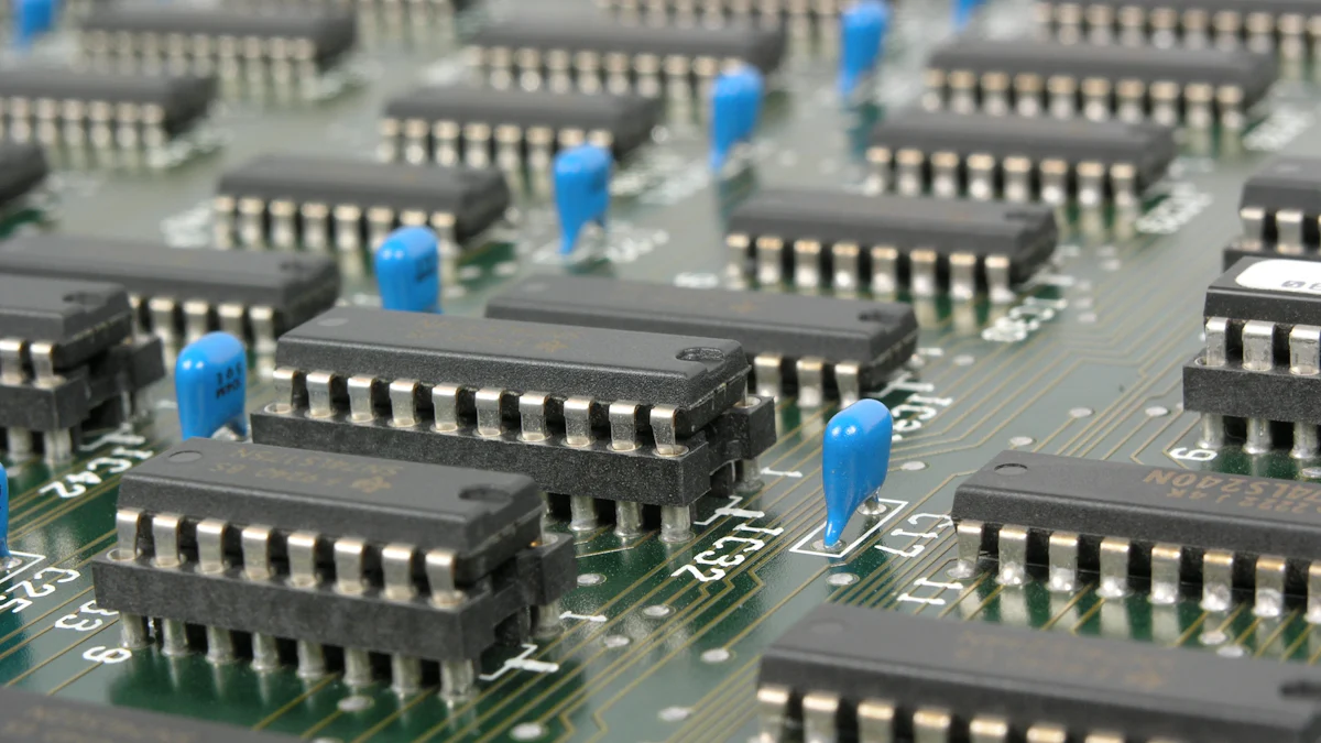
MM74HC4049N components and modules

The MM74HC4049N components are a CMOS hex buffer/inverter IC featuring six independent channels. Each channel is designed to invert the input signal, ensuring reliable logic operations. This IC supports a voltage range of 2 V to 6 V and operates efficiently with a maximum propagation delay of 15 ns. The MM74HC4049N components are essential in high-speed, low-power digital circuits.
Key Specifications:
| Specification | Value |
|------------------------------|---------------------------|
| Voltage Supply Range | 2 V ~ 6 V |
| Number of Inputs | 6 |
| Operating Temperature Range | -40°C ~ 85°C |
| Current Quiescent Max | 2μA |
| Current Output High/Low | 5.2mA |
| Max Propagation Delay | 15ns @ 6V, 50pF |
| Logic Type | Inverter |
| Logic Level Low | 0.5 V ~ 1.8 V |
| Logic Level High | 1.5 V ~ 4.2 V |
Key Takeaways
- The MM74HC4049N is a useful CMOS hex buffer/inverter. It works well with voltages from 2V to 6V. This makes it great for many digital circuits.
- It uses very little power, only 2 μA when idle. This makes it perfect for devices that run on batteries. It helps batteries last longer while still working well.
- This chip is great for changing logic levels and buffering signals. It helps different circuits with different voltages work together easily.
Overview of MM74HC4049N Components
CMOS Technology and Internal Design
The MM74HC4049N components rely on CMOS technology, which enhances their performance and versatility. This technology allows the IC to function as a logic level translator, converting high-level logic signals to low-level ones. It operates efficiently with a low supply voltage, making it suitable for circuits with varying voltage levels. The internal design includes a modified input protection structure, enabling input voltages to exceed the supply voltage safely. A lower zener diode protects the IC from static voltages, ensuring reliability in diverse applications.
Internally, the MM74HC4049N features a hex inverter configuration, meaning it contains six independent inverting channels. This design supports high-speed operations with a typical propagation delay of 15 ns at 6V. The IC is housed in a 16-DIP package, which simplifies integration into your circuit designs.
| Feature | Specification |
|---|---|
| Configuration | Hex inverter |
| Voltage Supply Range | 2 V to 6 V |
| Max Propagation Delay | 15 ns at 6V |
| Quiescent Current | 2 μA |
| Package Type | 16-DIP |
| Operating Temperature Range | -40°C to 85°C |
Input and Output Characteristics
The MM74HC4049N components exhibit robust input and output characteristics, making them ideal for digital circuits. The IC supports a wide voltage supply range of 2V to 6V, ensuring compatibility with various systems. Its logic level thresholds are well-defined, with a low range of 0.5V to 1.8V and a high range of 1.5V to 4.2V. These thresholds allow the IC to handle diverse input signals effectively.
The output stage features a push-pull configuration, delivering a maximum current of 5.2 mA. This ensures strong signal driving capability, even in demanding applications. The IC's low quiescent current of 2 μA minimizes power consumption, making it suitable for energy-efficient designs.
| Parameter | Value |
|---|---|
| Voltage Supply Range | 2V to 6V |
| Maximum Propagation Delay | 15ns at 6V, 50pF |
| Logic Level Low Range | 0.5V to 1.8V |
| Logic Level High Range | 1.5V to 4.2V |
| Output Current (High/Low) | 5.2mA |
| Operating Temperature | -40°C to 85°C |
| Number of Elements | 6 |
| Logic Type | Buffer, Non-Inverting |
| Output Type | Push-Pull |
Voltage Levels and Power Requirements
The MM74HC4049N components operate within a voltage supply range of 2V to 6V, making them compatible with both low- and high-voltage systems. The IC's power requirements are minimal, with a maximum quiescent current of just 2 μA. This low power consumption ensures efficient operation in battery-powered devices and other energy-sensitive applications.
The IC's output current capability of 5.2 mA allows it to drive multiple loads without compromising performance. Its ability to handle varying voltage levels makes it a versatile choice for interfacing between different voltage domains.
| Specification | Value |
|---|---|
| Voltage Supply Range | 2 V to 6 V |
| Maximum Quiescent Current | 2 μA |
| Current Output (High/Low) | 5.2 mA |
MM74HC4049N Modules
Logic Level Shifting
The MM74HC4049N plays a vital role in logic level shifting. It converts high-level logic signals to low-level ones while operating from a low logic supply. This feature is essential when working with systems that use different voltage levels. The IC employs advanced silicon-gate CMOS technology, which ensures high performance and reliability. Its modified input protection structure allows the input voltage to exceed the supply voltage. This capability makes it an excellent choice for effective logic level translation in modern electronic designs.
Signal Buffering
Signal buffering is another key function of the MM74HC4049N. The IC strengthens weak signals, ensuring they can travel longer distances or drive multiple loads without degradation. With its push-pull output configuration, the IC delivers a maximum current of 5.2 mA. This strong driving capability makes it suitable for demanding applications. Additionally, its low quiescent current of 2 μA ensures minimal power consumption, which is ideal for energy-efficient designs.
Voltage Domain Interfacing
The MM74HC4049N excels in voltage domain interfacing, a critical requirement in complex systems. It acts as a logic level translator, converting high-level logic to low-level logic while using a low logic supply. This feature allows you to interface circuits operating at different voltage levels seamlessly. The IC's advanced CMOS technology and input protection structure enhance its versatility. You can use it as a logic level translator, a simple buffer, or an inverter, depending on your application needs.
| Feature | Details |
|---|---|
| Number of Inputs | 6 |
| Voltage Supply Range | 2V to 6V |
| Logic Type | Inverter |
| Max Propagation Delay | 15ns @ 6V, 50pF |
| Operating Temperature Range | -40°C ~ 85°C |
| Current Output High/Low | 5.2mA |
| Quiescent Current Max | 2μA |
Tip: The MM74HC4049N components simplify your design process by offering reliable logic level shifting, signal buffering, and voltage domain interfacing in one package.
Applications of MM74HC4049N
Microcontroller Interfacing
The MM74HC4049N simplifies microcontroller interfacing by acting as a hex inverter and logic level translator. It converts high-level logic signals to low-level ones, ensuring compatibility between devices operating at different voltage levels. This IC works seamlessly with CMOS logic and can also function as a simple buffer or inverter. Its wide power supply range (2V to 6V) and low quiescent current (20 µA maximum) make it ideal for energy-efficient designs. With a typical propagation delay of 8 ns, it supports high-speed applications, ensuring reliable performance in time-sensitive systems.
You can use the MM74HC4049N in various microcontroller-based projects, such as portable electronics, connected peripherals, and enterprise projectors. Its versatility and efficiency make it a valuable addition to your digital designs.
Signal Processing in Digital Circuits
The MM74HC4049N plays a crucial role in signal processing by ensuring compatibility between different voltage levels. It functions as a hex inverting logic level down converter, using advanced silicon-gate CMOS technology. This IC translates high-level logic signals to low-level ones, making it essential for circuits that require seamless communication between components.
| Feature | Description |
|---|---|
| Functionality | Hex inverting logic level down converter |
| Technology | Advanced silicon-gate CMOS technology |
| Purpose | Logic level translator for high-to-low signals |
| Application | Ensures compatibility in digital circuits |
You can rely on the MM74HC4049N to maintain signal integrity in complex systems, such as consumer electronics, medical devices, and industrial automation.
Battery-Powered Devices
The MM74HC4049N components are perfect for battery-powered devices due to their low power consumption. With a quiescent current of just 2 µA, this IC minimizes energy usage, extending battery life in portable electronics. Its ability to operate within a wide voltage range (2V to 6V) ensures compatibility with various power sources.
In addition to energy efficiency, the IC’s strong output current (5.2 mA) allows it to drive multiple loads without performance loss. This makes it suitable for applications like wearable devices, remote sensors, and other portable systems. By incorporating the MM74HC4049N, you can create designs that balance performance and power efficiency.
Note: The MM74HC4049N is widely used across industries, including automotive, renewable energy, and AI, due to its versatility and reliability.
Advantages and Limitations
Benefits of Using the MM74HC4049N
The MM74HC4049N offers several advantages that make it a valuable component in digital electronics.
- High-Speed Performance: With a maximum propagation delay of 15 ns, this IC ensures fast signal processing. You can rely on it for time-sensitive applications.
- Low Power Consumption: Its quiescent current of just 2 μA makes it ideal for energy-efficient designs, especially in battery-powered devices.
- Wide Voltage Range: The IC operates between 2V and 6V, allowing you to use it in both low- and high-voltage systems.
- Versatility: It functions as a logic level translator, signal buffer, and inverter. This flexibility simplifies your circuit designs.
- Strong Output Drive: The IC delivers up to 5.2 mA of output current, enabling it to drive multiple loads effectively.
Tip: The MM74HC4049N is perfect for projects requiring reliable logic level shifting and signal buffering.
Constraints and Limitations in Certain Applications
While the MM74HC4049N excels in many areas, it has some limitations you should consider.
- Limited Output Current: Although 5.2 mA is sufficient for most applications, it may not meet the needs of high-power systems.
- Temperature Sensitivity: Operating temperatures range from -40°C to 85°C. Extreme environments may affect its performance.
- Inverting Logic Only: The IC only provides inverting logic. If your design requires non-inverting logic, you may need additional components.
- Static Sensitivity: Despite its input protection, the IC remains sensitive to static discharge. Proper handling is essential.
Note: Understanding these constraints helps you decide if the MM74HC4049N fits your project requirements.
The MM74HC4049N stands out as a versatile and efficient component in digital electronics. Its wide voltage range, low power consumption, and fast propagation delay make it ideal for logic level translation, buffering, and interfacing.
| Feature | Description |
|---|---|
| Voltage Supply Range | 2V to 6V |
| Quiescent Supply Current | 20 µA maximum |
| Propagation Delay | 8 ns |
| Fanout | 10 LS-TTL loads |
| Compatibility | Pin and functionally compatible with CD4049BC |
| Applications | Logic level translation, simple buffer/inverter |
You can simplify your designs and enhance performance by incorporating this IC into your projects. Its reliability and flexibility make it a valuable tool for modern electronic systems. Explore its potential to elevate your designs today!
FAQ
What is the primary function of the MM74HC4049N?
The MM74HC4049N acts as a hex inverter. It converts high-level logic signals to low-level ones. It also buffers signals to ensure reliable performance in digital circuits.
Can you use the MM74HC4049N for voltage level translation?
Yes, you can use it for voltage level translation. It supports a wide voltage range (2V to 6V) and ensures compatibility between circuits with different voltage levels.
How does the MM74HC4049N benefit battery-powered devices?
The MM74HC4049N consumes minimal power (2 μA quiescent current). This feature extends battery life, making it ideal for portable electronics and energy-efficient designs.
Tip: Always check the voltage supply range and logic level compatibility before integrating the MM74HC4049N into your project.
See Also
Key Applications and Insights on the 74HC00DR
Specifications Overview of XC95144XL-10TQG144C Xilinx PLD
Three Primary Applications of LMH0302SQ in HD-SDI