What are the manufacturing processes of the latest MM74HC245AN?

The MM74HC245AN stands out as a high-speed CMOS octal bus transceiver. You might wonder how this component achieves its reliability and performance. Manufacturers rely on precise manufacturing processes to create it. These include advanced techniques that ensure every unit meets strict quality standards, making it a trusted choice for electronic applications.
Key Takeaways
- The MM74HC245AN is made using careful processes for top performance.
- Cutting the silicon wafer into pieces is called wafer dicing.
- This step is important to keep the circuits working well.
- Encapsulation shields the MM74HC245AN from damage caused by the environment.
- This makes it stronger and able to handle tough conditions.
Wafer Fabrication in Manufacturing Processes
Semiconductor Material Selection
The foundation of the MM74HC245AN begins with selecting the right semiconductor material. Manufacturers typically use silicon due to its excellent electrical properties and abundance. You might find it interesting that silicon wafers undergo a purification process to remove impurities. This ensures the material meets the high standards required for electronic components. The purified silicon is then sliced into thin wafers, which serve as the base for the entire manufacturing process.
Photolithography and Etching Techniques
Photolithography plays a critical role in shaping the intricate patterns on the silicon wafer. During this step, manufacturers coat the wafer with a light-sensitive material called photoresist. A mask with the desired circuit pattern is placed over the wafer, and ultraviolet light transfers the pattern onto the photoresist. Afterward, etching removes the unwanted material, leaving behind the precise circuit design. This process ensures the MM74HC245AN achieves its high-speed performance.
Did you know? Photolithography can create patterns as small as a few nanometers, enabling the production of compact and efficient components.
Deposition and Doping Steps
Deposition involves adding thin layers of materials onto the wafer to form the necessary structures. Techniques like chemical vapor deposition (CVD) or physical vapor deposition (PVD) are commonly used. After deposition, doping introduces impurities into specific areas of the wafer to modify its electrical properties. This step is crucial for creating the transistors and other elements that make up the MM74HC245AN. By carefully controlling these steps, manufacturers ensure the component's reliability and functionality.
Die Preparation and Inspection
Wafer Dicing into Individual Dies
Once the wafer fabrication process is complete, the next step involves dividing the wafer into individual dies. This process, known as wafer dicing, uses a high-precision diamond saw or a laser cutter. You might find it fascinating that these tools can cut through the wafer with incredible accuracy, ensuring minimal damage to the delicate circuits.
During dicing, manufacturers carefully align the wafer to ensure each die is separated along predefined scribe lines. These lines are etched onto the wafer during earlier stages of production. The precision of this step is critical because even a slight misalignment can render the dies unusable.
Tip: The size of each die depends on the complexity of the circuit. Smaller dies often indicate more advanced manufacturing techniques.
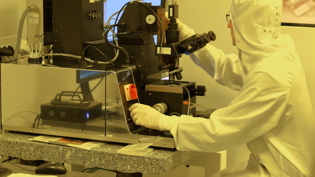
Quality Checks and Die Inspection
After dicing, each die undergoes a thorough inspection to ensure it meets quality standards. You might wonder why this step is so important. It helps identify defects like cracks, contamination, or misaligned circuits that could affect the component's performance.
Manufacturers use advanced tools like optical microscopes and automated inspection systems to examine the dies. These tools can detect even microscopic flaws. Once the inspection is complete, only the dies that pass all quality checks move forward in the manufacturing process.
By ensuring each die is flawless, manufacturers guarantee the reliability and performance of the MM74HC245AN in real-world applications.
Packaging in Manufacturing Processes
Lead Frame Attachment
The packaging process begins with attaching the die to a lead frame. This frame acts as the structural base and provides electrical connections for the MM74HC245AN. Manufacturers use a die attach adhesive or solder to secure the die to the frame. You might find it interesting that this step requires extreme precision. Misalignment can disrupt the electrical pathways, affecting the component's performance.
The lead frame also helps dissipate heat generated during operation. This ensures the MM74HC245AN remains reliable under various conditions. By carefully attaching the die, manufacturers set the stage for the next steps in the packaging process.
Encapsulation and Molding
Encapsulation protects the die and lead frame from environmental factors like moisture, dust, and physical damage. During this step, manufacturers place the assembly into a mold and inject a liquid epoxy resin. Once the resin hardens, it forms a durable shell around the component.
This protective layer ensures the MM74HC245AN can withstand harsh conditions. You might notice that the final product has a smooth, black exterior. This is the result of the encapsulation process.
Note: Encapsulation not only protects the component but also enhances its durability and longevity.
Wire Bonding for Electrical Connections
Wire bonding connects the die to the lead frame, enabling electrical signals to flow through the component. Manufacturers use ultra-thin gold or aluminum wires for this process. These wires are bonded to the die and lead frame using heat, pressure, or ultrasonic energy.
You might be amazed to learn that these wires are thinner than a human hair. Despite their size, they play a crucial role in the MM74HC245AN's functionality. Proper wire bonding ensures the component performs as intended in electronic circuits.
By completing these packaging steps, manufacturers ensure the MM74HC245AN is ready for testing and final assembly. These manufacturing processes highlight the precision and care involved in creating reliable electronic components.
Testing and Quality Control
Electrical Functionality Testing
Electrical functionality testing ensures the MM74HC245AN performs as intended. During this step, manufacturers evaluate the component's electrical characteristics, such as voltage levels, current flow, and signal integrity. Automated test equipment (ATE) plays a key role here. It runs a series of tests to verify that the transceiver meets design specifications.
You might find it interesting that these tests simulate real-world operating conditions. This ensures the component can handle the demands of various electronic applications. By identifying any issues early, manufacturers prevent defective units from reaching customers.
Environmental and Stress Testing
Environmental and stress testing evaluates how the MM74HC245AN withstands extreme conditions. Manufacturers expose the component to high and low temperatures, humidity, and mechanical stress. These tests reveal how the transceiver performs under challenging environments.
For example, thermal cycling tests simulate rapid temperature changes. This helps identify potential weaknesses in the material or design. Vibration tests ensure the component remains reliable during physical shocks. By conducting these tests, manufacturers guarantee the durability and longevity of the MM74HC245AN.
Note: Stress testing is crucial for ensuring the component's reliability in critical applications, such as industrial or automotive systems.
Final Defect Inspection
The final defect inspection serves as the last checkpoint in the manufacturing processes. Manufacturers use advanced imaging tools and automated systems to detect any remaining defects. These inspections focus on identifying issues like surface cracks, misaligned connections, or contamination.
You might wonder why this step is so important. It ensures only flawless components move forward to distribution. By maintaining strict quality control, manufacturers uphold the high standards expected of the MM74HC245AN.
Final Assembly and Distribution
Labeling and Marking
The final assembly process begins with labeling and marking the MM74HC245AN. Manufacturers use laser etching or ink printing to add essential details to the component's surface. These details include the part number, manufacturing date code, and batch information. You might notice that these markings are small but highly precise. They help you identify the component and trace its origin if needed.
Labeling ensures that the MM74HC245AN complies with industry standards. It also makes it easier for you to integrate the component into your designs. By adding clear and durable markings, manufacturers ensure the component remains identifiable throughout its lifecycle.
Packaging for Shipment
Packaging plays a critical role in protecting the MM74HC245AN during transportation. Manufacturers use anti-static packaging with electrostatic discharge (ESD) protection to shield the component from damage. This ensures the transceiver arrives in perfect condition.
The packaging also features 40% light transparency, allowing you to identify the component without opening the package. Durable construction provides Faraday Cage performance, which blocks external electrical interference. Before shipment, manufacturers inspect the goods to confirm they meet datasheet specifications.
| Specification/Assessment | Details |
|---|---|
| Packaging Type | Anti-static packaging with ESD protection |
| Transparency | 40% light transparency for easy identification of components |
| Construction | Durable buried metal construction providing Faraday Cage performance |
| Inspection | Goods inspected before shipment to ensure good condition and compliance with datasheet |
| Shipment Method | Global express delivery services (DHL, FedEx, TNT, UPS) |
| Resistance | Excellent puncture and tear resistance with good seal integrity |
This robust packaging ensures the MM74HC245AN reaches you securely, no matter where you are.
Distribution to Customers
Once packaged, the MM74HC245AN is ready for distribution. Manufacturers partner with global express delivery services like DHL, FedEx, and UPS to ship the components worldwide. These services ensure fast and reliable delivery, so you can receive the product on time.
Distribution networks also include authorized distributors and online platforms. This makes it easy for you to access the MM74HC245AN, whether you need a single unit or bulk quantities. By streamlining the distribution process, manufacturers ensure the component reaches you efficiently and in excellent condition.
The manufacturing processes of the MM74HC245AN showcase the complexity and precision required to create reliable electronic components. Each step, from wafer fabrication to final distribution, ensures the transceiver’s high performance. These processes reflect the innovation behind semiconductor manufacturing, even for components that may no longer be cutting-edge.
FAQ
What makes the MM74HC245AN reliable for electronic applications?
Manufacturers use precise processes like photolithography, wire bonding, and stress testing. These steps ensure durability, high performance, and reliability in various environments.
How does encapsulation protect the MM74HC245AN?
Encapsulation shields the component from moisture, dust, and physical damage. It also enhances durability by forming a tough epoxy resin shell around the die and lead frame.
Why is wafer dicing important in manufacturing?
Wafer dicing separates the wafer into individual dies. Precision during this step ensures minimal damage to circuits, which is critical for the component's functionality.
💡 Tip: Always source components from authorized distributors to ensure quality and authenticity.
See Also
Key Applications and Insights on the 74HC00DR Chip
Detailed Specifications of the XC95144XL-10TQG144C PLD
Role of C8051F340-GQR in Industrial Automation Systems
Harnessing Video Processing Capabilities with GS2972-IBE3
Essential Information About CP2104-F03-GMR in Embedded Systems