the manufacturing processes of the latest MM74HC4050N

The MM74HC4050N stands out as a high-speed CMOS hex buffer, designed to handle voltage level shifting and signal buffering in electronic circuits. You can rely on its advanced manufacturing processes to deliver exceptional performance and reliability. These processes include precise raw material preparation, cutting-edge semiconductor fabrication, and meticulous assembly. Each step ensures the component meets strict industry standards. The final product undergoes rigorous quality control, guaranteeing its durability and efficiency in various applications. With its robust design, the MM74HC4050N remains a trusted choice for modern electronic systems.
Key Takeaways
- The MM74HC4050N is a high-speed CMOS hex buffer that efficiently handles voltage level shifting and signal buffering in electronic circuits.
- With a voltage range of 2V to 6V, this device is versatile and suitable for various applications, enhancing circuit stability and reliability.
- The manufacturing process emphasizes precision, starting from high-quality raw materials like semiconductor-grade silicon to ensure optimal performance.
- Advanced fabrication techniques, including photolithography and etching, are crucial for creating the intricate patterns that define the MM74HC4050N's functionality.
- Rigorous quality control and testing procedures guarantee that each MM74HC4050N meets strict performance standards before reaching consumers.
- The robust design and low power consumption of the MM74HC4050N make it an ideal choice for both engineers and hobbyists looking to create efficient electronic systems.
- Understanding the manufacturing processes of the MM74HC4050N can help you appreciate the technology behind reliable semiconductor devices.
Overview of the MM74HC4050N
Purpose and Functionality
The MM74HC4050N serves as a vital component in electronic circuits. You can use it to shift voltage levels and buffer signals, ensuring smooth communication between different parts of a circuit. This hex buffer operates efficiently within a voltage range of 2V to 6V, making it versatile for various applications. It plays a key role in protecting sensitive components by isolating them from high-voltage signals. By incorporating this device, you can enhance the stability and reliability of your electronic systems.
This buffer also simplifies circuit design. It reduces the complexity of managing voltage differences between components. Its ability to handle high-speed operations ensures that your circuits perform optimally, even in demanding environments. Whether you're working on consumer electronics or industrial systems, the MM74HC4050N provides the functionality you need.
Key Features and Benefits
The MM74HC4050N offers several features that make it a standout choice for engineers and hobbyists alike. Here are some of its key attributes:
- High-Speed Performance: You can rely on its fast switching capabilities to maintain efficient signal processing in your circuits.
- Wide Voltage Range: Its compatibility with voltages from 2V to 6V allows you to use it in a variety of applications without worrying about compatibility issues.
- Low Power Consumption: This device minimizes energy usage, helping you design power-efficient systems.
- Robust Design: Its durable construction ensures long-term reliability, even under challenging conditions.
- Ease of Integration: The MM74HC4050N's straightforward design makes it easy for you to incorporate it into your projects.
"The MM74HC4050N is a CMOS buffer that operates within a voltage range of 2V to 6V, making it suitable for various electronic applications." – Industry Insights
By choosing the MM74HC4050N, you gain access to a reliable and efficient solution for voltage level shifting and signal buffering. Its features not only simplify your design process but also improve the overall performance of your electronic systems.
Raw Materials and Preparation
The manufacturing processes of the MM74HC4050N begin with selecting and preparing high-quality raw materials. These materials form the foundation of the component's performance and reliability. By understanding the importance of each material, you can appreciate the precision and care involved in creating this advanced semiconductor device.
Semiconductor Materials
You need to start with semiconductor-grade silicon, which serves as the primary material for the MM74HC4050N. Manufacturers use silicon due to its excellent electrical properties and availability. This material undergoes rigorous testing to ensure it meets strict purity standards. Impurities can disrupt the functionality of the final product, so maintaining high purity is essential.
In addition to silicon, other materials like dopants play a critical role. Dopants modify the electrical properties of silicon, enabling it to function as a semiconductor. These substances include elements such as phosphorus and boron. By carefully controlling the type and amount of dopants, manufacturers can create the desired electrical characteristics for the MM74HC4050N.
Material Preparation
Once the raw materials are selected, you must prepare them for the next stages of production. Silicon wafers are created by slicing purified silicon crystals into thin, circular discs. Each wafer undergoes polishing to achieve a smooth surface, which is crucial for the subsequent fabrication steps. A clean and defect-free wafer ensures the accuracy of the intricate patterns etched during the manufacturing processes.
Dopants are introduced during this stage to create specific regions within the silicon wafer. This process, known as doping, involves diffusing or implanting dopant atoms into the silicon. The precise placement of these atoms determines the electrical behavior of the semiconductor. You can think of this step as setting the foundation for the MM74HC4050N's functionality.
Manufacturers also apply protective coatings to the wafers to shield them from contamination. These coatings preserve the integrity of the material during handling and storage. By maintaining strict cleanliness standards, you can ensure that the prepared materials are ready for the complex fabrication process that follows.
Fabrication Process
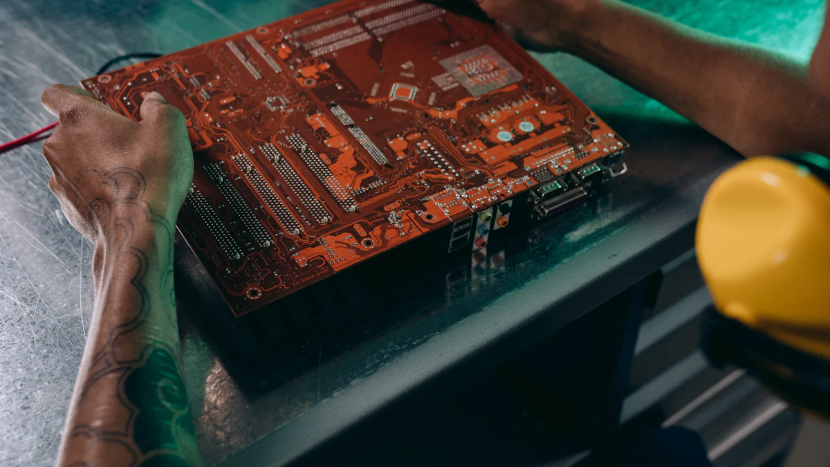
The fabrication process transforms prepared materials into functional semiconductor devices. You will find this stage critical in defining the performance and reliability of the MM74HC4050N. Each step requires precision and advanced technology to achieve the desired results.
Wafer Processing
Wafer processing begins with the silicon wafers prepared earlier. You will see these wafers undergo cleaning to remove any contaminants. This ensures a pristine surface for the intricate patterns that will be created. Photolithography follows, where you use light to transfer circuit patterns onto the wafer. A photosensitive material, called photoresist, coats the wafer. You expose it to ultraviolet light through a mask that contains the circuit design. The exposed areas of the photoresist harden, while the unexposed areas remain soft and removable.
Afterward, you develop the wafer to reveal the circuit pattern. This step sets the foundation for the electrical pathways within the MM74HC4050N. The precision of this process directly impacts the device's functionality. You must ensure accuracy at this stage to avoid defects in the final product.
Etching and Deposition
Etching removes unwanted material from the wafer to create the desired circuit structure. You can use either wet etching, which involves chemical solutions, or dry etching, which uses plasma. Both methods allow you to carve out precise patterns on the wafer. The choice of technique depends on the complexity of the design and the required level of detail.
Deposition follows etching. In this step, you add thin layers of material to the wafer. These layers form the various components of the semiconductor. Techniques like chemical vapor deposition (CVD) and physical vapor deposition (PVD) help you achieve uniform and high-quality layers. Each layer contributes to the overall functionality of the MM74HC4050N. You must carefully control the thickness and composition of these layers to meet the device's specifications.
Finalizing the Semiconductor
The finalization stage brings all the elements together. You will see the wafer undergo doping again to refine its electrical properties. This step ensures that the semiconductor regions function as intended. After doping, you apply a protective layer to shield the wafer from damage during subsequent handling.
Next, you divide the wafer into individual chips through a process called dicing. Each chip represents a single MM74HC4050N device. You inspect these chips to identify any defects. Only those that meet the strict quality standards proceed to the next stage. This ensures that every MM74HC4050N delivers reliable performance in its applications.
The fabrication process combines precision, technology, and expertise. By mastering these manufacturing processes, you can create high-quality semiconductor devices like the MM74HC4050N.
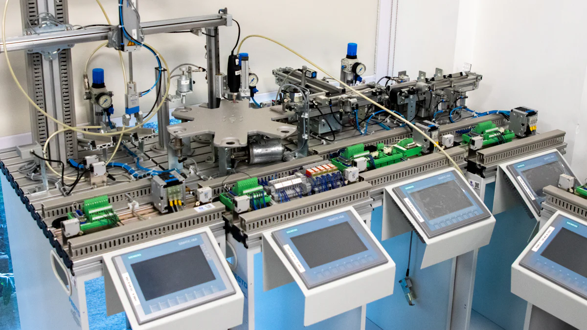
Assembly and Packaging
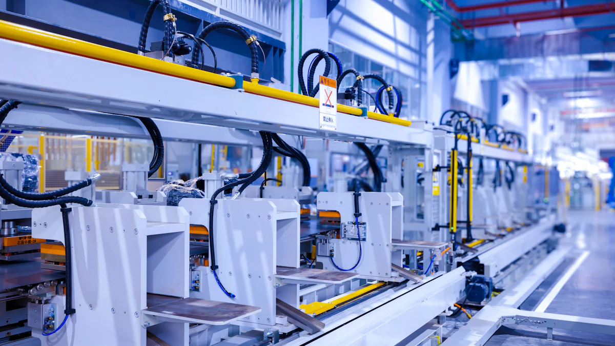
The assembly and packaging stages play a crucial role in transforming the fabricated semiconductor chips into a finished product ready for use. These steps ensure that the MM74HC4050N is not only functional but also durable and protected during handling, transportation, and application.
Component Assembly
In the component assembly stage, you will see the individual semiconductor chips, created during the fabrication process, integrated with other essential elements. This step involves mounting the chips onto a substrate or lead frame, which serves as the foundation for electrical connections. Manufacturers use advanced techniques like soldering and adhesive bonding to secure the chips in place. These methods ensure a strong and reliable connection, preventing any movement or damage during operation.
Wire bonding follows the mounting process. Thin gold or aluminum wires connect the chip's internal circuitry to the external pins or leads. This step allows the MM74HC4050N to interface with other components in an electronic circuit. Precision is critical here, as even a minor misalignment can affect the device's performance. Automated machines handle this task to achieve consistent and accurate results.
After wire bonding, manufacturers encapsulate the assembled components in a protective material. This material shields the delicate internal structures from environmental factors like moisture, dust, and mechanical stress. By the end of this stage, the MM74HC4050N takes on its recognizable form, ready for the final packaging process.
Packaging Process
The packaging process ensures that the MM74HC4050N is safe and secure for storage, transportation, and eventual use. You will notice that manufacturers prioritize both functionality and presentation during this stage. The packaging not only protects the product but also provides essential information for users.
First, the assembled components are placed in anti-static bags. These bags prevent electrostatic discharge (ESD), which can damage sensitive electronic devices. The anti-static packaging includes labels with key details such as the part number, brand, and quantity. This information helps you identify the product easily and ensures traceability throughout the supply chain.
Next, the packaged components are organized into boxes or trays for bulk handling. Structural packaging designs, such as those offered by companies like JohnsByrne, optimize space and provide additional protection. Some manufacturers also include final gluing, inserting, or kitting services to enhance the packaging's durability and usability.
Finally, the products undergo a thorough inspection to verify that the packaging meets quality standards. This step ensures that every MM74HC4050N reaches you in perfect condition, ready to deliver reliable performance in your electronic projects.
"All the products will be packed in an anti-static bag with ESD antistatic protection." – Industry Standard Practice
The assembly and packaging stages highlight the importance of precision and care in the manufacturing processes. By focusing on these steps, manufacturers ensure that the MM74HC4050N remains a trusted choice for engineers and hobbyists alike.
Quality Control and Testing
The quality control and testing phase ensures that every MM74HC4050N meets the highest standards of performance and reliability. You will find this stage essential in identifying and eliminating defects, guaranteeing that the final product functions as intended in various applications.
Testing Procedures
Testing begins with a series of precise and systematic evaluations. Manufacturers use advanced equipment to assess the electrical properties of each semiconductor chip. These tests verify that the device operates within its specified voltage range of 2V to 6V and performs its buffering and voltage-shifting functions effectively. Automated testing systems handle this process to ensure consistency and accuracy across all units.
You will notice that manufacturers often employ Shewhart control charts during testing. These charts help monitor the performance of the testing equipment and detect any deviations from expected results. By analyzing these charts, you can identify potential issues early and take corrective actions to maintain the integrity of the manufacturing processes.
Functional testing follows the initial evaluations. This step simulates real-world conditions to confirm that the MM74HC4050N performs reliably under various scenarios. For example, the device undergoes stress tests to evaluate its durability in high-speed operations. These tests ensure that the component can withstand demanding environments without compromising its functionality.
Quality Assurance Measures
Quality assurance focuses on maintaining strict standards throughout the production cycle. You will see manufacturers implement measures like Westgard stopping rules to ensure that testing remains accurate and reliable. These rules establish thresholds for acceptable performance, allowing you to halt production if results fall outside the defined limits. This proactive approach minimizes the risk of defective products reaching the market.
Calibration plays a crucial role in quality assurance. Manufacturers regularly calibrate their testing instruments to maintain precision. Regression analysis helps identify trends and patterns in test data, enabling you to refine the manufacturing processes and improve overall product quality. By continuously monitoring and adjusting these processes, you can ensure that every MM74HC4050N meets industry standards.
Inspection is another vital aspect of quality assurance. Trained professionals examine the physical and functional aspects of the device to detect any flaws. This step includes visual inspections to identify surface defects and detailed analyses to verify internal structures. Only components that pass these rigorous checks proceed to packaging and distribution.
"Proposed methods utilizing Shewhart control charts, Westgard stopping rules, and regression analysis for instrument calibration and population sampling during data collection." – Quality Control Methodology for Data Collection in Epidemiologic Studies
By prioritizing quality control and testing, manufacturers uphold the reliability and performance of the MM74HC4050N. These measures ensure that you receive a product that meets your expectations and performs flawlessly in your electronic projects.
The manufacturing processes of the MM74HC4050N demonstrate the importance of precision and innovation. Each step, from material preparation to quality control, ensures you receive a reliable and high-performing component. These advanced techniques highlight how modern technology creates semiconductor devices that meet the demands of today’s electronics. By understanding these processes, you can appreciate the effort and expertise involved in delivering a product that supports your electronic projects with consistency and efficiency.
FAQ
What is the MM74HC4050N used for?
The MM74HC4050N serves as a hex buffer designed for voltage level shifting and signal buffering. You can use it to ensure smooth communication between different components in electronic circuits. It also protects sensitive parts by isolating them from high-voltage signals.
What voltage range does the MM74HC4050N support?
This device operates efficiently within a voltage range of 2V to 6V. Its wide compatibility makes it suitable for various applications, from consumer electronics to industrial systems.
How does the MM74HC4050N improve circuit performance?
The MM74HC4050N enhances circuit performance by reducing voltage mismatches between components. Its high-speed operation ensures efficient signal processing, while its low power consumption helps you design energy-efficient systems.
What materials are used to manufacture the MM74HC4050N?
Manufacturers use semiconductor-grade silicon as the primary material. Dopants like phosphorus and boron modify the silicon's electrical properties. Protective coatings are also applied to maintain material integrity during production.
What is the significance of doping in the manufacturing process?
Doping introduces specific impurities into the silicon wafer to alter its electrical properties. This step allows you to create regions within the semiconductor that perform distinct functions, ensuring the MM74HC4050N operates as intended.
How is the MM74HC4050N tested for quality?
Manufacturers conduct rigorous testing using advanced equipment. These tests evaluate electrical properties, functionality, and durability under real-world conditions. Only components that meet strict quality standards proceed to packaging and distribution.
What packaging methods are used for the MM74HC4050N?
The MM74HC4050N is packaged in anti-static bags to prevent electrostatic discharge. Labels provide essential details like part numbers and quantities. The final packaging ensures the product remains safe during storage and transportation.
Can the MM74HC4050N withstand harsh environments?
Yes, the MM74HC4050N features a robust design that ensures long-term reliability. Its protective encapsulation shields it from environmental factors like moisture, dust, and mechanical stress.
Why is precision important in the manufacturing process?
Precision ensures that each step, from material preparation to assembly, meets exact specifications. This accuracy minimizes defects and guarantees that the MM74HC4050N performs reliably in your applications.
Where is the MM74HC4050N manufactured?
The MM74HC4050N has been manufactured using advanced techniques, with significant production processes carried out in Great Britain. This origin reflects its high-quality standards and reliable performance.
See Also
Exploring Key Uses of the 74HC00DR Logic Gate
Harnessing SEMTECH's Video Processing Capabilities with GS2972-IBE3
Discovering the Efficiency of the LM5088MHX-2 Regulator